Relevant concepts
Contents
Relevant concepts#
Voltage Divider#
A Voltage Divider is a simple circuit to achieve a certain voltage, when only a higher voltage is available.
It uses the principle of a voltage drop across a resistor.
As shown in the figure above, its just two resistors in series, and the output is taken from the bottom two wires that exit to the right (the upper one is the reduced Voltage, the lower one Ground).
The formula is given as follows: Vout = R2/(R1 + R2) * Vin where R1 is the upper Resistor and R2 the lower one.
ADC#
ADC stands for Analog to Digital Converter. These kind of ICs are used where the analog world meats a Digital Processor or in this case FPGA.
ADCs convert an analog Voltage into a digital Signal to be processed by the FPGA.
The ADC communicates with the FPGA (or Micro Controller) via a communication protocol like SPI or I2C.
In this work a MCP3201 is used, which is a single channel 12bit ADC that communicates over SPI. The SPI Bus is explained in the following segment.
SPI#
SPI is a common communication bus to communicate with peripherals like sensors. It has 5 major connections:
Vin
Ground
MOSI (SDO from Master perspective) - Master Out Slave In
MISO (SDI from Master perspective) - Master In Slave Out
CS (CS as an inverted enable signal for the Device) - Chip Select
MOSI and MISO are shared data lines when multiple sensors are present, whereas every sensor gets its own CS line.
The master, in this case the FPGA, controls the communication and chooses with which bus user it wants to communicate with, by pulling its CS Pin Low.
The used ADC in this project sends its data on MISO as soon as CS gets pulled low, without needing a request from the master (FPGA).
Operational Amplifier#
An operational Amplifier does what its name implies - it amplifies. Different surrounding circuits can make it a very flexible building block.
In this project it is simply used to amplify the voltage difference that occurs when the Resistance of the Temperature Element changes and thus the voltage of the voltage divider changes.
Open Collector IO / Tach Signal of Fan#
The Open Collector Input Output Pins, are often used in Micro Controllers or ICs.
When active the device simply turns on an internal Mosfet, and connects the Pin to ground.
Open Collectors are often used in combination with an external or internal Pull-Up Resistor. The Voltage level the Pull-Up Resistor is connected to, can then be chosen to not exceed the maximum of the listening device.
In this project, the fans have Open Collector Pins on the Tach signal. The Voltage is then pulled up to 3.3V in Hardware with a 10k Pull-Up Resistor.
This way the Fan outputs a 3.3V to Ground PWM Signal which is readable by the FPGA.
The received signal frequency also has to be divided in half, because the magnetic sensor in the Fan gets activated twice per Rotation of the fan.
PT1000#
A PT1000 is a resistive temperature element (RTD). It changes its resistance approximately linearly with temperature what makes the conversion simple.
The changing resistance can be converted into a voltage via the previously explained voltage divider.
The 1000 in PT1000 stands for 1000 Ohm Resistance at 0°C.
Clock Divider#
Clock dividers do what their names imply and turn a higher frequency clock into a lower frequency one.
Clock dividers are most often implemented in software. Their simplest implementation is to use a counter and use the output from the third digit as its new clock (1:8 Clock divider). Here an intentional overflow is used to "reset" the counter.
Alternatively, for a more precise clock the counter can be checked if it has achieved a certain value. If so the counter is reset. In this project mostly this approach is used.
Seven Segment Display#
A Seven Segment Display is a Display with only 7 (or 8 with decimal point) inputs. It is used most often used to Display (hexadecimal) numbers or error codes, by illuminating different segments.
For a more in depth information on Seven Segment Displays on the boolean board check out the boolean Board Reference Manual
PMod#
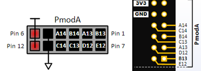
The PMod interface is a way to connect external peripherals to the boolean board. For this work the PModA connector of the boolean board was used.

For more information check out the boolean Board Reference Manual
The reference manual was used to get information about the pinout, which had to be used in the constraint file.
